Flexible electronics promises new morphological freedoms for active electronic systems. Circuits fabricated on flexible substrates can conform to curved surfaces, span large areas, and integrate sensing, computation, communication, powering and actuation directly within a single physical structure. Such systems may enable electronic skins for robotics, distributed environmental sensing surfaces, wearable or implantable biomedical devices, and even sustainable or biodegradable electronics. The ability to fabricate large-area electronics using printing or thin-film processes also opens the possibility of integrating electronics economically across surfaces that would be impractical using conventional silicon integrated circuits.
However, the materials and devices used in flexible electronics differ substantially from those used in conventional silicon CMOS technology. Thin-film transistor (TFT) technologies commonly used in flexible electronics include oxide semiconductors such as indium gallium zinc oxide (IGZO) and organic semiconductors. Each of these device families typically provide only one reliable transistor polarity. IGZO processes reliably produce n-type devices but lack high-performance p-type counterparts, while many organic semiconductor systems provide reasonably good p-type devices but relatively poor n-type devices. As a consequence, the complementary device pairing that underpins CMOS circuit design is generally unavailable.
The absence of complementary devices presents a fundamental challenge for translating established CMOS circuit design techniques to flexible electronics. Most modern analogue and mixed-signal circuits rely on complementary pull-up and pull-down networks to achieve high gain, large signal swings, and energy-efficient switching. Historically, digital electronics was implemented using unipolar logic families such as NMOS logic before the widespread adoption of CMOS in the late 1970s. In contrast, modern neuromorphic circuits have almost exclusively been developed in CMOS technologies, and the design motifs of neuromorphic systems—such as synaptic integrators, spiking neurons, and address-event communication circuits—have been formulated assuming the availability of complementary transistors.
Neuromorphic systems represent an especially attractive computational paradigm for flexible electronics (Delbruck and Liu 2010; Indiveri et al. 2011). Spiking neural networks process information using sparse event-driven signals and analogue temporal dynamics, enabling energy-efficient computation and natural integration with sensory transduction. Furthermore, neuromorphic architectures map naturally onto spatially distributed sensing systems, making them appealing for large-area sensing substrates and robotic skins. However, the circuit primitives used to implement these systems in CMOS have not been systematically translated to unipolar transistor technologies.
In this work we investigate how core neuromorphic circuit motifs can be implemented using a modern unipolar thin-film process. Specifically, we focus on circuits designed using n-type thin-film transistors from Pragmatic Semiconductor’s FlexIC process, which provides IGZO devices together with resistive pull-up elements but no complementary p-type transistors. We demonstrate that the essential components required for an end-to-end mixed-signal spiking neural network can be realised within this constraint.
An additional architectural opportunity arises from the mechanical properties of flexible electronic substrates. Three-dimensional integration is already widely used in silicon electronics, for example through die stacking and through-silicon vias in modern vision sensors and memory devices. However, these structures are typically fixed during fabrication and rely on specialised manufacturing processes. In contrast, flexible electronic systems can be assembled, stacked, or mechanically modified after fabrication using relatively simple processes. This enables multilayer circuit structures in which conductive traces on adjacent flexible layers may interact through capacitive coupling across the thin dielectric substrates separating them.
In this work we explore the novel use of such capacitive coupling as a mechanism for transmitting spiking signals between layers of a neuromorphic network. Spikes propagating along axonal pathways on one flexible layer can be capacitively coupled into receiving circuits on neighbouring layers, enabling inter-layer communication without vertical vias or rigid interconnect structures. This mechanism is an architectural affordance that arises naturally from flexible substrates and is particularly compatible with neuromorphic systems, where information is represented by transient spike events rather than static voltage levels.
To support this architecture we develop circuit designs compatible with a unipolar thin-film process that implement the core functional elements of a spiking neural network. These include spiking transduction from analogue signals, capacitive axonal signal transmission, log-domain synaptic integration, and leaky integrate-and-fire (LIF) neuronal dynamics. Simulations are performed using the Pragmatic FlexIC Hellvelyn 1.2 design kit.
Together, these results demonstrate that the essential building blocks of mixed-signal neuromorphic systems can be implemented using a modern unipolar thin-film process. This provides a pathway for integrating sensing, computation, and communication within large-area flexible electronic substrates.
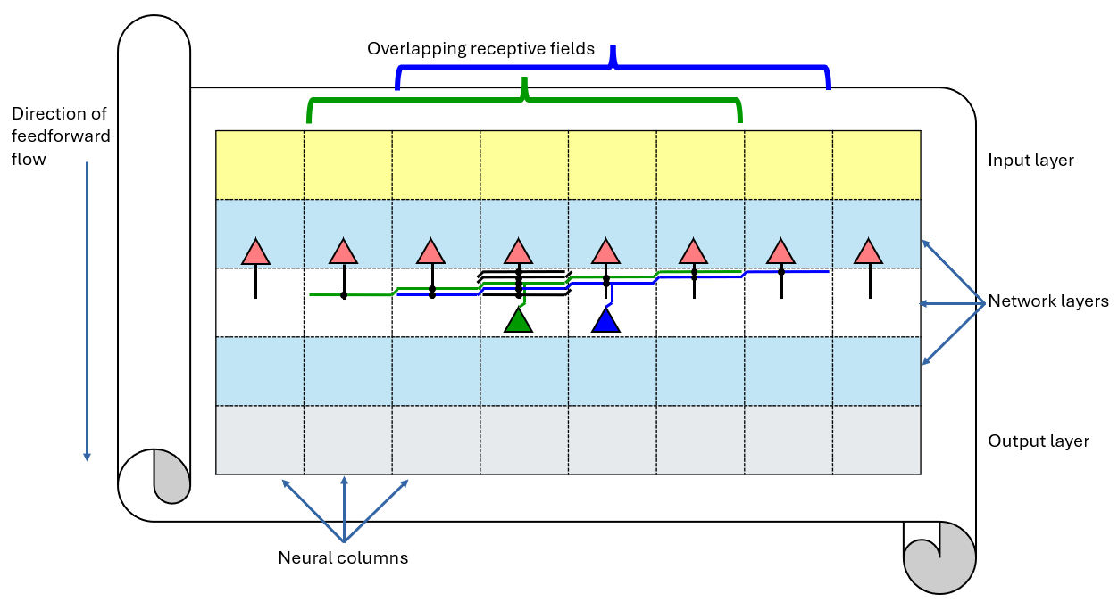
The neuromorphic system considered in this work is organised as a set of repeating processing units distributed across a flexible electronic sheet. Figure 1 illustrates the overall layout of such a system. Processing elements are arranged laterally across the flexible substrate as a series of neural columns, which form the fundamental structural units of the architecture. In the example shown, eight columns are arranged side by side in this example, although in practice the number of columns is determined by the physical width of the flexible substrate and the dimensions of the circuit blocks that implement each neuron.
The architecture is organised vertically into an input layer, a sequence of network layers (3 in this example), and a final output layer. Signal flow proceeds in a feed-forward direction from the top of the structure toward the bottom (although recurrent (lateral or feedback) connections could also be designed). Each network layer contains one neuron per column together with the synaptic circuitry required to receive spikes generated by neurons in the preceding layer.
Communication between layers occurs through axonal wires that propagate spikes from one layer to the next. The axon of each neuron carries voltage pulses downward to the synaptic array of the subsequent layer. Within this array, axons intersect with horizontal dendritic wires associated with neurons in the receiving layer. Each dendritic wire corresponds to a particular neuron in that layer and collects synaptic currents generated by spikes arriving from multiple presynaptic axons.
At each intersection between an axon and a dendrite, a synapse circuit converts voltage pulses travelling along the axon into current pulses injected into the dendritic wire. These junctions are indicated by black dots in Fig. 1. The resulting current pulses propagate along the dendrite and are integrated by the synaptic integrator associated with the target neuron.
Because dendritic wires extend laterally across multiple columns, neurons can receive input from presynaptic neurons located in neighbouring columns. The lateral extent of the dendritic wiring therefore determines the receptive fields of neurons within each layer. Two example dendrites are illustrated in full in Fig. 1, shown in green and blue, corresponding to the neurons indicated by matching coloured triangles. The repeating connection pattern is illustrated for column four using short black segments. This pattern produces overlapping receptive fields spanning five neighbouring columns, as indicated by the braces above the diagram.
The diagram shows three network layers for illustration, although additional layers can be added to increase network depth. At the base of the structure, neurons in the final layer form the output layer, whose spike outputs may be transmitted onward either to additional processing stages or to external communication interfaces. The internal structure of the neural column used to implement each of these processing units is now described.
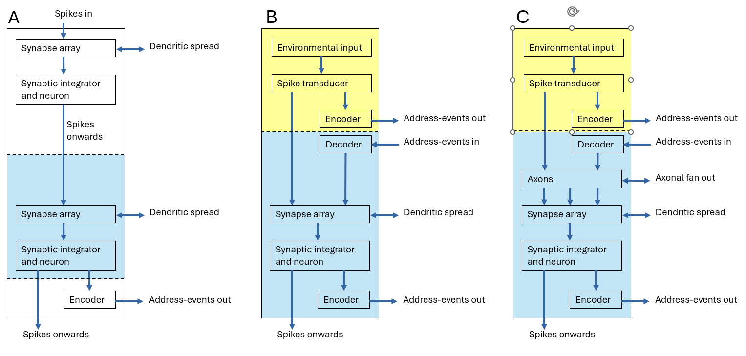
Figure 2 illustrates a generic neuromorphic “column” architecture that forms the basic repeating motif of the proposed system. The term column is used here purely as a structural design unit rather than as a reference to biological cortical columns. Each column represents a vertical chain of processing stages that may be replicated laterally across a flexible substrate to construct larger networks.
In its simplest form (Fig. 2A), the column consists of a sequence of layers through which spike signals propagate along axonal connections. Spikes enter the top of the column from an upstream source and are transmitted downward along axonal pathways to a synaptic array. The synaptic array is implemented as a crossbar structure in which axons run vertically while dendritic lines run horizontally. At each axon–dendrite intersection a synapse circuit converts incoming voltage spikes on the axon into current pulses injected into the dendrite. The dendritic wires collect these synaptic currents and deliver them to a synaptic integrator, which performs a low-pass filtering operation before driving the membrane node of a leaky integrate-and-fire neuron. When the membrane potential crosses threshold the neuron emits an output spike which may propagate onward to subsequent layers of the network.
The crossbar arrangement naturally supports lateral communication between neighbouring columns. While axons propagate spikes vertically through successive layers, dendritic wires extend horizontally across adjacent columns, allowing synaptic fan-in and fan-out between neurons located in neighbouring columns. The width of the flexible substrate therefore determines the number of neurons that can be accommodated within each layer. Lateral dendritic connectivity may be either global or spatially restricted, allowing the construction of local receptive fields and projective fields along the horizontal dimension of the substrate.
In the simplest configuration (Fig. 2A), columns can be stacked vertically to form feed-forward layers. Two such layers are shown in the diagram, although additional layers may be appended above or below. Spikes generated by neurons in one layer propagate along axons to the synaptic array of the next layer. At the base of the column, spikes may either continue propagating into further layers or be routed to an address-event encoder for multiplexed communication with other regions of the system.
Figure 2B illustrates a more general column architecture in which each layer may serve both as an entry point and an exit point for spike events. In this configuration a decoder at the input of the layer receives address-event signals and reconstructs local spikes, while an encoder at the output converts locally generated spikes into address-event packets for transmission elsewhere in the system. In parallel with this multiplexed communication pathway, spikes may still propagate directly along axonal connections between successive layers. The upper section of Fig. 2B additionally illustrates how sensory functionality may be incorporated into the column. Environmental signals are first transduced into analogue electrical signals and then converted into spike events by a spike-generation circuit. These spikes form the input to the first synaptic processing stage. The environmental input may originate from a variety of transducers integrated on the flexible substrate, including mechanical sensors (for example capacitive or piezoelectric structures), chemically functionalised sensing surfaces, or photodetectors.
Finally, Fig. 2C introduces a third architectural capability enabled by flexible substrates: spike transmission between layers of flexible material. In addition to lateral fan-out through dendritic connections, spikes may also be transmitted vertically between stacked strata through capacitive coupling. This can be achieved by forming conductive plates on neighbouring flexible strata that align to create capacitors whose dielectric is the flexible substrate itself. Pulses on an axonal line in one stratum capacitively couple to detection circuits in an adjacent stratum, which then regenerate and drive new axonal spikes into the local synaptic array. Allowing spikes to propagate between a limited number of neighbouring strata in this way enables receptive and projective fields to extend across a second spatial dimension corresponding to the stacking direction of the flexible strata. (We distinguish between layers, which denote neural network layers in the computational sense, and strata, which denote physically distinct flexible substrates stacked in the third dimension).
Together, these column architectures illustrate how large neuromorphic networks can be constructed from repeated circuit motifs implemented in a unipolar thin-film transistor process while exploiting the structural properties of flexible substrates.

We first describe the circuits necessary for excitation, in the vertically central band of Fig.3, describing first the synapses then the synaptic integrator then the neuron. Each dendritic synapse receives spike events from a dedicated axonal wire. From the perspective of the neuron, these spikes arrive as digital voltage pulses applied to the gate of transistor Mpulse. The pulses are of short, controlled duration, typically in the range of 100μs - 1 ms. When activated, Mpulse allows current to flow through a second transistor Mweight whose gate is biased by ngbWeight. Each synapse has its own weight bias, so the weight of the first excitatory synapse is denoted ngbWeightExc1. This bias sets the strength of the synaptic connection. In the present work the origin of this bias voltage is not specified; it could be generated by a variety of local analogue memory mechanisms compatible with thin-film processing, including charge-trapping TFT memories, floating-gate structures, ferroelectric devices, or resistive switching elements reported in oxide semiconductor technologies such as IGZO (Nomura et al. 2004; Kamiya and Hosono 2010; Park, Kim, et al. 2012; Kwon et al. 2014; Park, Jeon, et al. 2012; Seo et al. 2011; Choi et al. 2014). These are not, however, available in the standard offering from PragmatIC.
The current pulses generated by individual synapses are injected onto a shared dendritic wire. Multiple synapses therefore contribute current to the same node, allowing synaptic currents to sum naturally. These currents are integrated by the synaptic conductance circuit, which implements a log-domain translinear structure extending from the synaptic devices to transistor Mconductance that couples the synaptic integrator to the neuron membrane. The effective integration capacitance is formed by Cconductance together with the source capacitances of the individual Mweight transistors. As a result, each synaptic input produces an exponentially decaying conductance kernel, with the dendrite node voltage representing the synaptic conductance logarithmically.
A leak path from the dendrite node is provided by transistor Mleak, whose gate is biased by the n-type gate bias ngbSynCondLeak. This device sets the baseline decay of synaptic conductance. To stabilise the lower operating point of the dendrite node, transistor Mreset connects the dendrite to the bias node nsbSynBaseline, which acts as a stabilised supply approximately 100 mV above ground. When the dendritic voltage approaches this level the effective source and drain of Mreset interchange, causing the device to conduct and oppose the leak current from Mleak. The dendrite voltage therefore stabilises slightly below nsbSynBaseline in the absence of synaptic input. This arrangement helps maintain a more linear leak characteristic in voltage, which produces the desired exponential decay in synaptic current. A more ideal diodic behaviour from Mreset would improve this characteristic.
The Mreset device can also optionally provide an active reset of the synaptic conductance. As shown in Fig. 3, the nsbSynBaseline bias may be applied to the gate of Mreset via the ground reference of inverter InvResetSyn. An active-low resetN pulse therefore forces the dendritic node toward the baseline voltage, resetting the synaptic conductance. Such resetting is useful for experimental protocols such as first-spike timing measurements, although typical biological neuron models do not require synaptic conductances to be reset following each output spike. In the simulations we present, we include InvResetSyn but resetN of the synaptic integrators remain at Vdd.
The synaptic conductance drives the neuron through transistor Mconductance, which pulls current from the neuron restingPotential node. This device also references the nsbSynBaseline node so that it is strongly turned off when the dendrite voltage approaches its minimum value.
The neuron membrane dynamics are implemented using capacitor Cmem connected between the membrane and restingPotential nodes. When an active-low resetN signal is applied, it is inverted by InvMemReset, turning on transistor MmemLeak and shorting the membrane and restingPotential nodes together. The equilibrium voltage reached during this reset phase is determined by the pair Mresting and Rresting, which form a bias network whose operating point occurs where the currents through the two devices are equal. Because the source of Mresting is connected to ground, the reset operation discharges the membrane capacitance Cmem.
Once the reset pulse ends, MmemLeak becomes weakly biased by the gate voltage ngbMemLeak through the ground connection of InvMemReset. During normal operation, synaptic activity pulls down the restingPotential node via Mconductance. As this occurs Mresting begins to turn off, producing a negative feedback loop mediated by Cmem. The membrane voltage rises as charge is redistributed across Cmem while the restingPotential node is held approximately constant. In this configuration the neuron behaves as a current-based leaky integrate-and-fire (CUBA-LIF) neuron, since the synaptic conductance depends only on synaptic input and is largely independent of the membrane voltage.
Spike generation is implemented using transistor Mthreshold and resistor Rthreshold, which are matched in size to Mresting and Rresting. Unlike Mresting, however, the source of Mthreshold is connected to the bias node nsbThreshold, which is raised above ground (approximately 200 mV in the simulations presented later). Under normal conditions the gate-to-source voltage of Mthreshold is therefore smaller than that of Mresting, and the output node spikeN remains high. When the membrane voltage rises sufficiently, Mthreshold begins to conduct and eventually pulls spikeN low, generating the spike event. This design resembles the second-stage amplifier of the dynamic vision sensor pixel (Lichtsteiner et al. 2008), however in contrast to such CMOS implementations that tune threshold using complementary transistor gate biases, here the effective threshold is adjusted by shifting the source potential of the active transistor.
Once the spike signal spikeN is generated, it may either trigger an axonal output pulse, initiate an address-event encoding sequence, or both. In either case the spike signal is typically sharpened using additional inverter stages. Furthermore, a reset pulse must be generated to restore the neuron state following a spike, either immediately or in response to acknowledgement from a communication circuit.
To generate pulses of controlled duration we employ monostable circuits. Each pulse that must be produced—such as the axon pulse or the reset pulse—is generated by a separate monostable so that their durations may be independently controlled. The monostable circuit is shown in the inset of Fig. 3. Transistor Min and Mfeedback together with resistor Rnand form a NAND structure that produces a short pulse on preCap when the input signal is asserted. This pulse is coupled through capacitor Cpulse to raise the node postCap. The node then decays through transistor Mduration at a rate set by the bias ngbDuration. The resulting waveform is inverted by InvMonostable to generate an active-low output pulse. The feedback transistor Mfeedback ensures that the duration of the output pulse is determined by the RC decay and is therefore independent of the duration of the triggering input pulse.
In the simplest configuration the signal spikeN passes through two inverter stages before branching into two monostables. One monostable generates the reset pulse resetN, while the other produces the outgoing axonal pulse, typically through an additional inverter stage to provide sufficient drive strength for fan-out along the axonal wire.
Inhibition is implemented using a second synaptic integrator, but in this case, the drain of MConductance is wired to Vdd and the source is wired to the RestingPotential of the neuron. nsbBaseline is driven by a separate source bias nsbDiffBaseline, which should be at the same voltage as restingPotential, and which to minimise temperature dependence should be constructed from a biasing structure which mirrors the resting branch (see section [sec:biasing] ). A separate set of synapses drive the inhibitory dendrite wire dendriteInh. In Fig. 3, axon1 is shown driving both the first excitatory and the first inhibitory synapse, suggesting two synapses per post-synaptic neuron per axon— a topological liberty which the brain doesn’t make much use of, according to Dale’s principle. When synaptic input raises dendriteInh above restingPotential, Mconductance sources current onto restingPotential which drives membrane downwards via the same feedback mechanism. This will straightforwardly counteract any rising of membrane due to the excitatory branch. However, if membrane starts to get driven downwards past restingPotential, Mreset becomes reverse-biased, starts to conduct and brings it back up again. This configuration gives us the liberty to set a different synaptic decay constant for excitatory and inhibitory branches by applying different biases, ngbSynCondLeakExc and ngbSynCondLeakInh respectively. Although each MConductance enjoys an approximately constant Vds, this Vds is different between the two branches. This and other differences such as numbers of connections can be resolved in the weighting of the individual synapses. In the simulations with multiple synapses which follow, we use one characteristic weight for all of the excitatory synapses and another for the inhibitory ones, ngbWeightExc and ngbWeightInh respectively.
A key requirement for large-area neuromorphic systems implemented on flexible substrates is the ability to convert a wide range of environmental signals into spike events in a modality-independent manner. In contrast to conventional pixel or sensor circuits, which typically measure absolute voltage or current levels, neuromorphic systems benefit from encoding temporal changes in signals as discrete events. This motivates the use of a spike transducer that responds directly to changes in charge at its input node, rather than to steady-state values. Such an approach allows a common circuit structure to be used across multiple sensing modalities, including piezocapacitive, photonic, chemical, or other transduction mechanisms, provided that the sensor produces a movement of charge in response to changes in the environment.
The spike transducer presented here in Fig. 4 converts charge variations at the input node in into two types of events, corresponding to the addition or removal of charge. These are denoted as flood and ebb, respectively, referring to the flow of positive charge into or away from the in node. The terminology is chosen to remain agnostic to the physical interpretation of the signal: depending on the sensing modality and biasing conditions, either polarity of event may correspond to an increase or decrease in the underlying stimulus. This differs from the conventional ON/OFF terminology used in dynamic vision sensors, which assumes a fixed relationship between signal polarity and physical meaning. For example, a piezo-capacitor presenting one plate to in and the other to Gnd, when squeezed, may produce either a flood or an ebb of charge at in, depending only on which way it has been polarised.
The core analogue circuit is derived from the second-stage differencing amplifier used in event-based vision sensors (Lichtsteiner et al. 2008), but adapted for a unipolar thin-film process. In particular, active pull-up devices are replaced with resistive loads, and threshold conditions are established through source biasing of n-type transistors rather than through complementary device pairs. Following a reset operation, transistor Mreset equalises the voltages at nodes in and diff, establishing an operating point in which the current through Mdiff is set by resistor Rdiff.
During normal operation, the input node in is held at a virtual ground by capacitive feedback between diff and in, implemented through capacitor Cfb. A change in charge at in perturbs this equilibrium, producing a voltage change at diff that is amplified according to the effective capacitance ratio. The gain of this stage is inversely proportional to Cfb, such that smaller capacitances produce larger voltage excursions at diff. In the limiting case, the intrinsic parasitic capacitances of the devices, in particular the drain-to-gate capacitance of Mdiff, may be sufficient to realise high gain without an explicit feedback capacitor. In the present work, simulations are performed using a 20 × 20 μm capacitor available in the FlexIC process, corresponding to approximately 1 pF.
Threshold detection is implemented through two branches connected to node diff, corresponding to the detection of flood and ebb events. These branches consist of transistors Mflood and Mebb with resistive loads, whose effective thresholds are determined by source bias voltages nsbDiff and nsbEbb. By arranging these biases such that nsbEbb > nsbDiff > ground, the circuit detects excursions of diff in both directions. When the perturbation exceeds the threshold of either branch, the corresponding output (flood or the active-low ebbN) undergoes a rapid transition, producing a quasi-digital event signal.
Two alternative input configurations are supported. In the direct configuration, the in node is driven directly by a charge source, such as a piezocapacitive sensor, and in simulations in this paper, this configuration is used, driven by an ideal current source. In this mode, reset transitions can couple back into the sensor, potentially introducing disturbance. To mitigate this, a buffered input pathway may instead be used, in which a voltage signal inPreBuffer is first buffered (for example using an n-type source follower) and then coupled to the in node through a feed-forward capacitor Cff. In this configuration the effective gain at diff is determined by the ratio −Cff/Cfb, and the sensor is isolated from reset-induced perturbations.
Programmable gain may in principle be achieved by replacing Cff and Cfb with banks of selectable capacitors. For example, capacitors connected to in could be selectively switched between inBuffered, diff, or a floating state to adjust the effective gain dynamically. Although not implemented here, such an approach is compatible with the proposed architecture.
When the total capacitance at node in becomes comparable to parasitic capacitances, reset-induced charge injection through Mreset can introduce a significant offset in the voltage at diff. This effect is mitigated by the inclusion of a dummy transistor Mdummy, driven by resetN, with both source and drain connected to in. This device injects a compensating charge during reset transitions, reducing feedthrough and improving repeatability. While this mechanism has been included in simulation, device sizing has not been optimised.
The outputs flood and ebbN are subsequently converted to a common active-high polarity by passing ebbN through a single inverter and flood through two inverter stages. These signals may then either drive axonal outputs directly or be routed to an asynchronous communication interface. To enable robust event handling and compatibility with quasi-delay-insensitive (QDI) logic, the signals are processed by a latching arbiter.
The latching arbiter performs two essential functions. Firstly, it converts transient input events into persistent states, latching the occurrence of an event until it is explicitly reset. Secondly, it resolves contention between competing inputs, ensuring that only one event is propagated when multiple inputs occur simultaneously or in rapid succession. This is achieved using two cross-coupled latching arbiter halves (LAH in Fig. 4), each associated with one polarity of event and inhibiting the other.
Each LAH is implemented as a pair of circularly coupled logic stages in which the output of one stage reinforces the state of the other, forming a stable latch. Consistent with the unipolar design approach, logic is realised entirely in the pull-down network, with resistive pull-ups providing the restoring force. The intermediate node qN represents the latched internal state, while the output node q is formed by resistor Rout and transistor Mout. Additional transistors Mblock and Mgrant (unusually, an n-type in the pull-up network), provide mutual exclusion and enable controlled switching of the output node.
During contention, the arbiter enters a metastable condition that resolves through the internal feedback structure, ensuring that only one output is asserted. This corresponds to the resolution of a mutual exclusion condition, a fundamental requirement for asynchronous event-driven systems. Additional inverter stages may be included at the outputs to meet the drive and logic-level requirements of downstream circuitry.
Following event detection and arbitration, the encoder should trigger a monostable circuit to generate reset signals. These reset signals, resetN and reset, both release the arbiter and restore the spike transducer to its initial state, enabling continuous operation.

In addition to lateral communication through dendritic wiring, the architecture supports vertical signal propagation between strata through axonal fan-out structures. Figure 5 illustrates the organisation of axonal bundles and the associated circuitry used to transmit and receive spike signals both within a stratum and across stacked flexible substrates.
A bundle of axons descends from the network layer above, carrying spike signals downwards toward the synaptic crossbar of the next network layer. Each axon is implemented as a wire with a pull-up resistor to Vdd, potentially allowing multiple sources to introduce active-low spike signals onto the same wire. An additional circuit block, referred to as the axon core, interfaces with these axons. Depending on its configuration, the axon core may detect a spike from the third dimension and if so, generate a reamplified spike that is inserted into a new axon in the bundle, as the bundle continues toward subsequent layers.
The behaviour of the axon core is controlled by a pair of configuration bits, send and receive, provided by a local configuration block. The method of storing these configuration bits is not specified in the present work; they may be realised using chains of latches, which can be created in the FlexIC process, or possibly through local non-volatile memory elements compatible with thin-film processing. The axon core is also connected to a large conductive plate, which is implemented as a metal region in the FlexIC process. In representative layouts not presented here, plates of approximately 400 × 400 μm are used, significantly larger than the associated circuitry, which occupies less than one quarter of this area.
These plates are aligned across multiple flexible strata, forming capacitive couplings in the third dimension, such as C1_2 shown between plates 1 and 2 in the diagram. When one plate is driven by a spike signal and another is configured to receive, the resulting electric field across the dielectric substrate allows spikes to be transmitted between layers without direct (ohmic) electrical connections. For well-aligned plates of area 400 × 400 μm separated by a dielectric thickness of approximately 30 μm and with relative permittivity ϵr ≈ 3, the resulting capacitance is approximately $$C_{\text{axon}} = \epsilon_0 \epsilon_r \frac{A}{d} \approx 8.85 \times 10^{-12} \times 3 \times \frac{(400 \times 10^{-6})^2}{30 \times 10^{-6}} \approx 0.14~\text{pF}.$$
Edge effects will contribute smaller capacitances, potentially coupling non-adjacent plates, as shown for example in the diagram by C2_4. Such edge effects are ignored for the following simulations.
The axon core operates in one of three modes depending on the configuration bits. When send is asserted, the circuit drives the plate node. Incoming active-low spikes on the axon are inverted and applied to transistor MspikeSend, which pulls the plate sharply toward ground for the duration of the spike. When the spike terminates, the plate voltage is restored toward Vdd through the series action of Mleak and Rdiff.
When receive is asserted, the plate node is left electrically floating with respect to strong drivers, and the receive circuitry establishes a neutral operating point. This neutral voltage is defined by the equilibrium between Mdiff and Rdiff, in a manner analogous to the biasing used in the spike transducer. The plate is gradually restored to this operating point through transistor Mleak, which is gated by the bias ngbAxonReset.
When a transient voltage is induced on the plate by capacitive coupling from a neighbouring layer, the receiver circuit responds through a feedback mechanism involving capacitor Cfb. The plate node is held near a virtual ground, while the voltage at the internal node diff rises in response with a gain proportional to −Caxon/Cfb. If this excursion exceeds the threshold defined by the Mthresh–Rthresh branch, a spike event is generated. This event is then shaped by a monostable circuit and used to produce an active-low output spike on the axon via transistor MspikeDown.
If neither send nor receive is asserted, the axon core operates in a blocking mode. In this configuration, the plate is actively anchored to ground through dedicated transistors, preventing the transmission of signals in the third dimension. These blocking transistors may require relatively large device sizes to provide strong anchoring, although device optimisation has not been explored in the present simulations.
The use of multiple plates within the same spatial region allows selective communication between layers. In the example shown in Fig. 5, plate 3 is configured to send while plate 2 is configured to receive, enabling signal transmission between those layers through the effective capacitance C2_3 = Caxon. Plates 1 and 4 are configured in blocking mode, anchoring their potentials to ground and thereby creating a neutral region in the electric field. This arrangement allows communication between selected layers while reducing unintended coupling to neighbouring structures, for example plate 5 is effectively shielded from plate 3 by plate 4, as the simulations will show.
While a complete routing architecture for axonal bundles and plate arrays is beyond the scope of the present work, the use of pull-up resistors on each axon ensures that multiple sources may safely introduce spikes onto a shared line. Together, these circuits demonstrate a mechanism for implementing controlled inter-layer communication in flexible neuromorphic systems using capacitive coupling rather than direct interconnects.
It will be apparent that there are significant possibilities for noise to couple onto the plates or from the plates to other circuits. However the plates are expected to align in different vertical zones from the circuits, and the axon node circuit is designed so that plate is the only floating node.
Simulations are performed in the Cadence - Virtuoso - Spectre stack, using Pragmatic’s Helvellyn PDK v1.2 (at the time of writing, Pragmatic have released a version 3.0 of this PDK, with significantly different device sizings). N-type source biases (nsb) are provided by ideal voltage sources, whereas N-type gate biases are created with an ideal current source driving through a diode-connected nmosfet, and the gate voltage is stabilised with an ideal buffer before being applied to the circuit. table 1 shows the nominal biases used unless otherwise stated; for gate biases, the current (prefix i) is given, rather than the resulting voltage.
| Circuit | Source biases | Gate biases | ||
| Name | Value (V) | Name | Value (pA) | |
| General | Vdd | 3.3 | iSpikeDuration | 2e3 |
| Synapse | iSynWeightExc | 1e4 | ||
| iSynWeightInh | 5e4 | |||
| Synaptic integrator | nsbSynapseBaseline | 0.1 | iSynCondLeakExc | 1e2 |
| iSynCondLeakInh | 5e1 | |||
| Neuron | nsbNeuronThresh | 0.2 | iMemLeak | 2e1 |
| iNeuronResetDuration | 2e3 | |||
| Spike transducer | nsbDiff | 0.25 | iNeuronResetDuration | 1e4 |
| nsbEbb | 0.35 | |||
| Axon | nsbAxonThresh | 0.6 | iAxonResetDuration | 2e2 |
| Circuit | Device | Size |
|---|---|---|
| General | Short n-type transistor | W: 5 μm; L: 800 nm |
| Long n-type transistor | W: 5 μm; L: 8 μm | |
| Synaptic Integrator | Cconductance | 110 × 47 μm2; 14 pF |
| Neuron | Cmem | 20 × 20 μm2; 1.1 pF |
| Monostable | Cpulse | 16 × 24 μm2; 1 pF |
| Spike Transducer | Cfb | 20 × 20 μm2; 1.1 pF |
| Axon | Cfb | 20 × 20 μm2; 1.1 pF |


The synaptic integrator is first simulated independently of the neuron, with restingPotential clamped at 500mV, being approximately the value that the neuron circuit produces at the nominal corner. Firstly the DC behaviour is explored, by providing a continuous current from a single synapse and sweeping both iWeight (0 - 10 nA) and iSynCondLeak (20 pA - 2 nA). Fig. 6 shows that the DC current which Mconductance sinks scales approximately linearly with iWeight, via the approximately logarithmic scaling of the DC dendrite voltage. Fig. 7 Shows the effect of iSynCondLeak on the DC conductance. We expect the relationship to be inversely proportional, and in fact the plot for 1 / iConductance versus iSynCondLeak is approximately linear, with the limitations of linearity apparent at the lower end of the iWeight range. The curve for zero iWeight is also given, showing the effective leakage current to the neuron for a synapse which is fully switched off - there are approximately 2 orders of magnitude difference up to our chosen maximum weight of 10nA.

The dynamic behaviour of the synaptic integrator is evaluated using transient simulations in which a single synapse is driven by a burst of input pulses, see figure 8. The input consists of a sequence of 1 ms wide pulses applied between t = −92 ms and t = 0 s, after which the input is removed to observe the decay of synaptic conductance. Three pulse periods are considered: 2 ms, 5 ms, and 10 ms, corresponding to duty cycles of 50%, 20%, and 10%, respectively.
During the stimulation phase, successive pulses accumulate on the synaptic integrator, producing a rising average conductance with a superimposed ripple at the pulse frequency. As expected, shorter pulse periods (higher duty cycle) result in a higher steady-state conductance, reflecting the balance between input-driven accumulation and leakage through Mleak. The amplitude of the ripple decreases as the pulse period increases, as the integrator has more time to decay between successive inputs.
The effect of the leak current iSynCondLeak is also evident. Lower values of iSynCondLeak (50 pA) result in higher steady-state conductance levels due to reduced leakage, while higher values (200 pA) limit accumulation and reduce the peak conductance. Following the cessation of input at t = 0, the conductance decays exponentially toward its baseline value, with the decay rate set by iSynCondLeak. Larger leak currents produce faster decay, consistent with the intended role of Mleak in controlling the synaptic time constant.
Overall, these results confirm that the synaptic integrator produces the expected behaviour of a current-based leaky integrator, with independently tunable gain and decay characteristics governed by the input pulse statistics and the leak bias.


The neuron is first demonstrated with a steady current sink in place of the synaptic integrator. Figure 9 shows the spike signal after a single inversion of the immediate spikeN neuron output. iSyn is swept through 3 orders of magnitude from 1 pA to 1 nA. Two different current biases are tried for the iResetDuration, i.e. the current bias of the monostable that generates the resetN signal, and therefore sets the refractory period. The resulting spike rates are plotted in figure 10 . A certain sustained synaptic current is necessary to overcome the neuron’s leak and achieve any spiking. Thereafter the spike rate takes off as iSyn rises, but in the case of iResetDuration = 2 nA, quickly asymptotes towards a maximum spike rate dominated by the refractory period, yielding a classic thresholded, saturating neuron transfer characteristic. With a shorter refractory period in the case of iResetDuration = 20 nA, the spike rate is able to go higher before the curve starts to flatten.

Figure 11 gives more insight into the behaviour of the neuron, showing an initial period in which a few spikes are produced. It can be seen that restingPotential is held at its nominal value except for brief disturbances at reset-release and spike events. membrane also has these disturbances, but during integration the signal rises. This rise creates an amplified fall in spikeN which ultimately triggers a digital swing in spike. resetN then lowers for a period which is dictated by the iResetDuration bias: 2 nA achieves a 1 ms refractor period whereas 20 nA achieves a 0.1 ms period.

Figure 12 shows the performance of a neuron driven by both excitatory and inhibitory synaptic integrators, as in figure 3. Each synaptic integrator has one synapse attached and the input spike streams are shown (axonExc, and axonInh). All spikes have a duration of 1 ms and all bursts have a duty cycle of 50%. A first excitatory burst starting at 20 ms raises dendriteExc and drive a burst of output spikes starting at 26 ms. When the burst stops at 39 ms, two further spikes occur until dendriteExc has decayed sufficiently that the excitatory synaptic current is no long sufficient - membrane subsequently lowers towards its resting level. A burst on axonInh from 60 ms to 79 ms raises dendriteInh, which hastens the flattening of the membrane trace. After this burst finishes, a second excitatory burst starts on axonExh at 80 ms, however, whereas the previous identical burst caused a first spike within 6 ms, this burst finds itself competing with the remaining inhibition from the inhibitory integrator, so that membrane creeps up only slowly, and the neuron eventually spikes 17 ms later. The neuron then reaches a stable firing pattern, until a further inhibitory burst arrives from 180 ms. Now the two bursts directly compete for control of the neuron and the membrane settles towards an intermediate level, too low to evoke further spikes. Finally, when all input spikes cease at 199 ms, the two dendrite traces return towards their resting states at characteristically different rates, controlled by the different biases (see table 1.
The spike transducer is demonstrated in figure 13 with a direct input driven by a sinusoidal current source. The output spikes are not passed through the latching arbiter but rather fed to a nor gate and then to a reset monostable, where the nor imitates either an instantaneous return from an event encoder or the case where spikes are consumed directly by subsequent neural layers rather than being encoded. While the current input sine-wave is positive, i.e. a flood of positive charge, the in node remains approximately at it’s virtual ground, whilst diff node accumulates the difference from a previously established reset level, until the flood node makes a positive transition, causing a spike, which can be seen at the output of the nor gate, i.e. the spikeN signal. This causes a reset signal which lasts 0.2 ms (resulting from the choice of iResetDuration bias), during which diff is held level with in. Thereafter the cycle repeats, with the spike rate increasing slightly towards the centre of the wave. When the wave transitions to its negative phase, i.e. an ebb of charge, this causes positive swings on diff w.r.t. its reset level, which cause negative transitions on the ebbN signal, also resulting in spikes. Although the flood and ebbN signals have quite different qualities, by the time these signals have been through a series of digital gates, any difference is the waveform of the spikeN signal is scarcely noticeable, and irrelevant for ongoing computation.
Figure 14 shows that spike rates for the two polarities can be modified by the voltage biases nsbDiff and nsbEbb, although they are not independent of each other: the flood spike rate depends primarily on the distance between nsbDiff and gnd, whereas the ebb spike rate depends primarily on the distance between nsbDiff and nsbEbb.
Drafting finishes here ...


Figure 16


SB Acknowledges helpful discussions with Ella Janotte, Simon Muller Cleve, David Verity, Alejandro, Simeone etc. AI has been used in the drafting of this document, and in the writing of some code for testbenches and analysis. The authors will vouch for the correctness of all the content once complete.
CB acknowledges the financial support of the National Biodiversity Future Center funded under the National Recovery and Resilience Plan (NRRP), Mission 4 Component 2 Investment 1.4 - Call for tender No. 3138 of 16 December 2021, rectified by Decree n.3175 of 18 December 2021 of Italian Ministry of University and Research funded by the European Union – NextGenerationEU. SB acknowledges the financial support from PNRR MUR Project PE000013 "Future Artificial Intelligence Research (hereafter FAIR)", funded by the European Union – NextGenerationEU.
.... and PRIMI ...
All authors declare no competing interests.
Not applicable.
Not applicable.
...
Not applicable.
Code can be found here:
...
SB ... CB ...