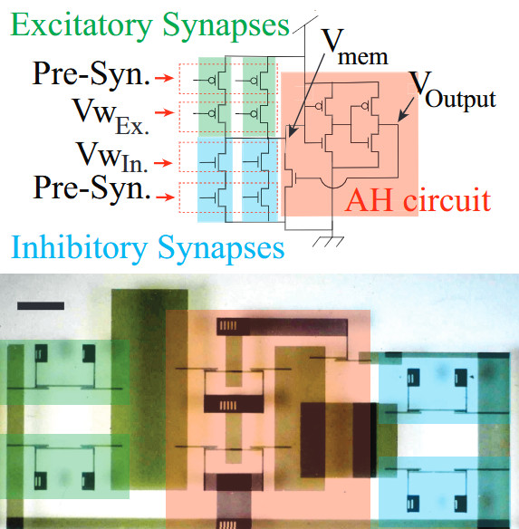
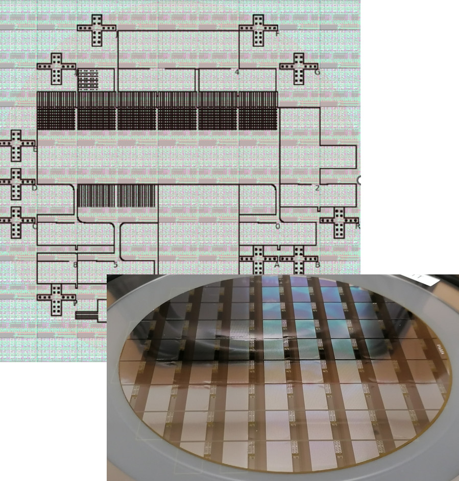
A test chip (X-Fab 180 nm) has been created with 3 different ways of transducing (piezo-)capacitive tactile signals into asynchronous digital spike trains (pdf).

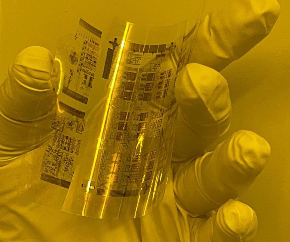
Together with colleagues at the Italian Institute of Technology, I've been exploring design possibilities at the junction between tactile sensing, neuromorphic engineering and flexible printed electronics. I've been designing for IGZO transistors and OTFTs, as well as silicon.
A test chip (X-Fab 180 nm) has been created with 3 different ways of transducing (piezo-)capacitive tactile signals into asynchronous digital spike trains (pdf).
An array of taxels embedding these modes has been fabricated (X-Fab 180 nm) and is awaiting test.
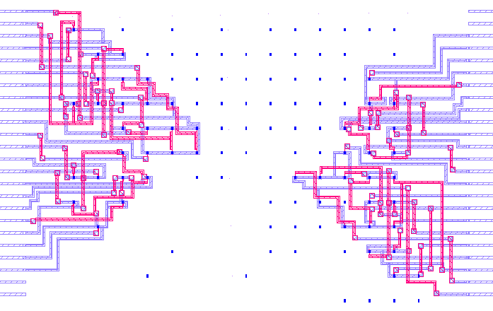
Design of an alternative system for encoding asynchronous events, that could be compatible with roll printing (pdf).
Blue-skies research question: could a 3D robotic nervous system roll out of a 2D printer?
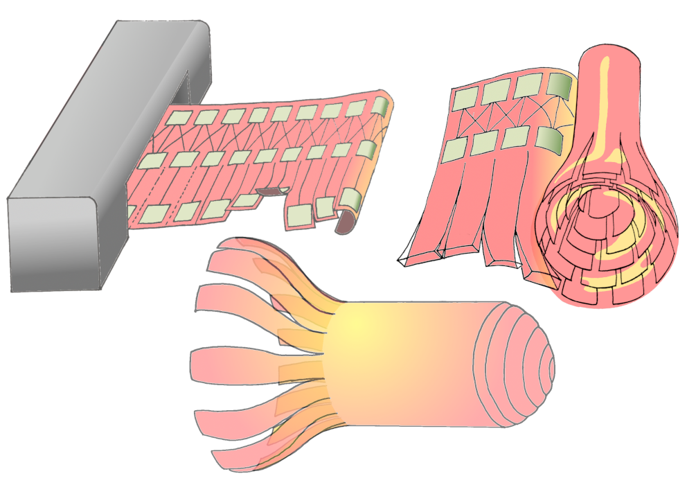
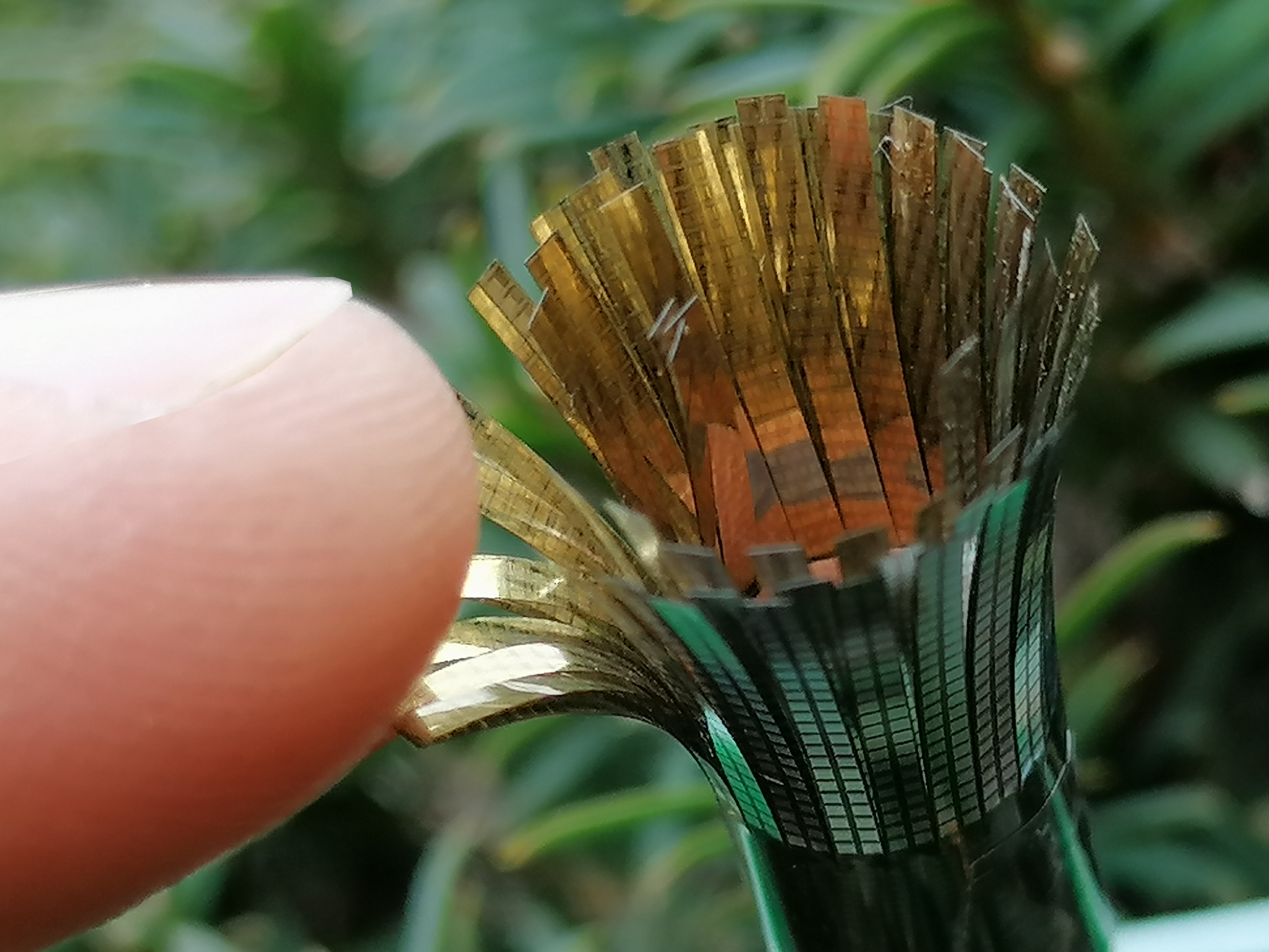
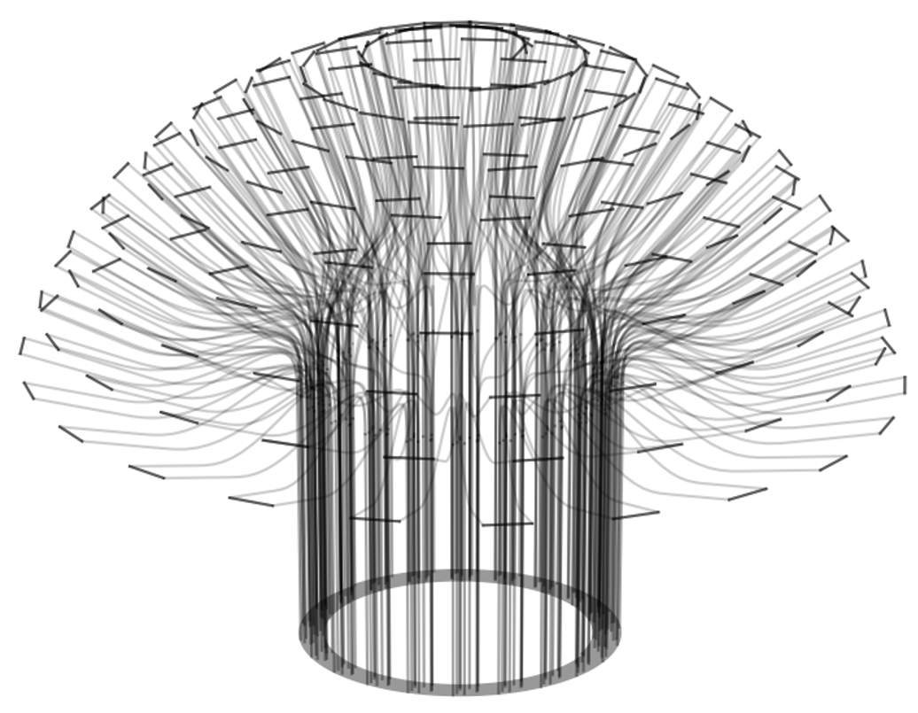
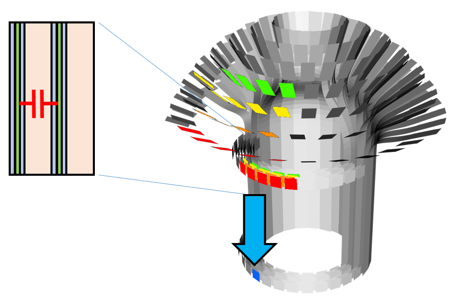
Coiled fanned sensor modelled and patented.
Dummy models created.
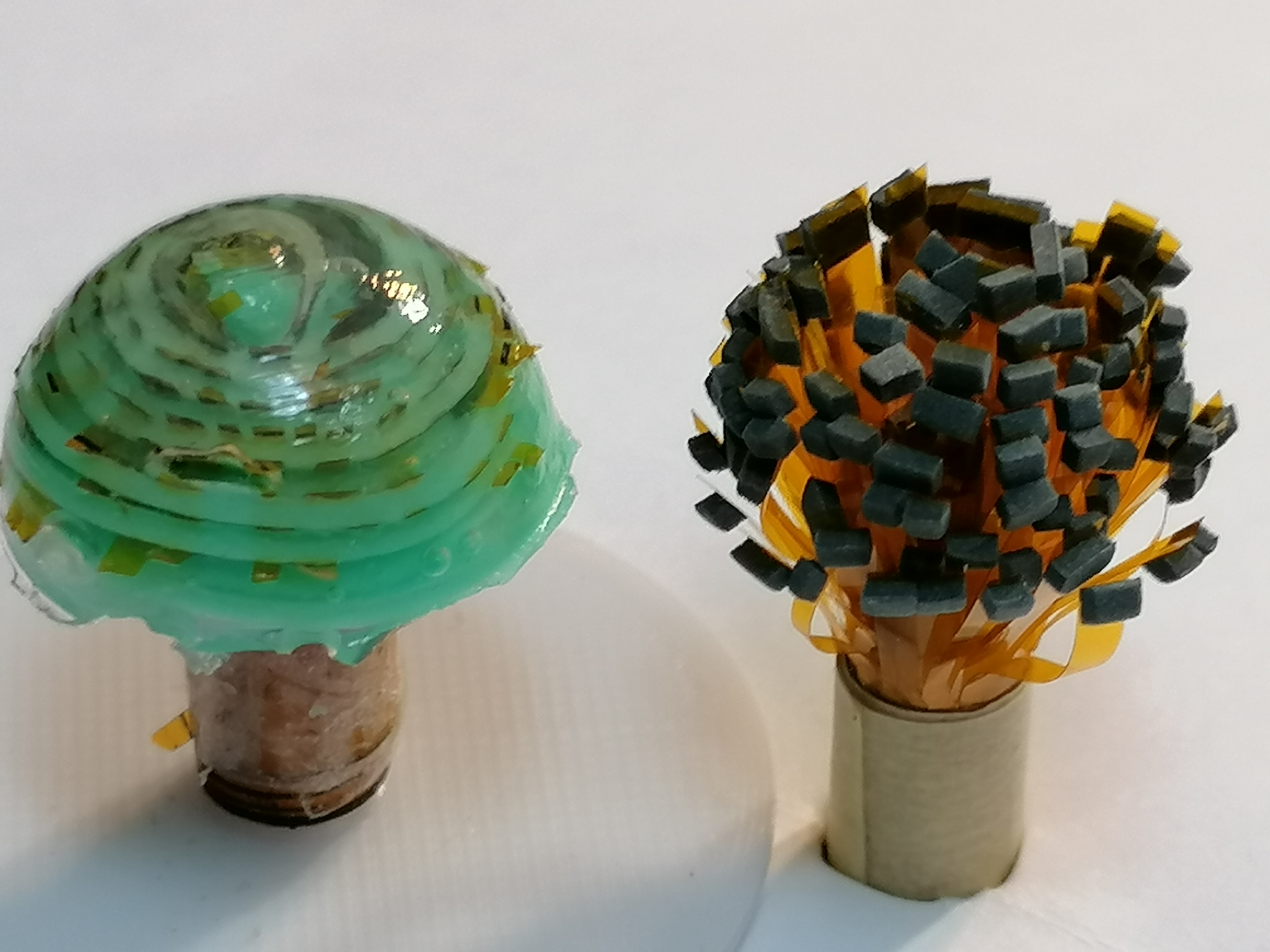
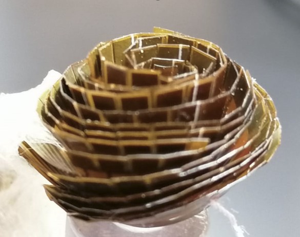
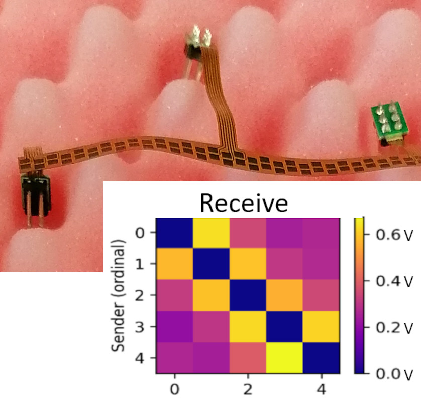
Coiled sensor fabricated using flex-PCB.
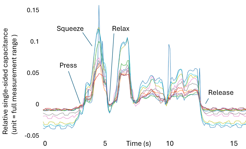
Basic capacitive sensitivity demonstrated (probing a patch where a subset of taxels have been sensorised externally).
Capacitive 'axonal' coupling between coiled layers, first experiments.
Single capacitive sensor circuit first proof of concept (Collaboration with Fleep).
Array integration attempted, but yield very poor.
3D 'axonal' communication through capacitive coupling between coiled layers, concept developed.
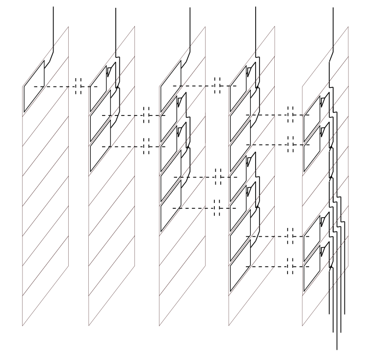
Modelling between circuits and topology.
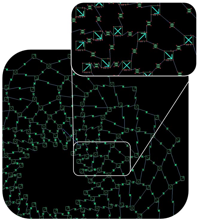
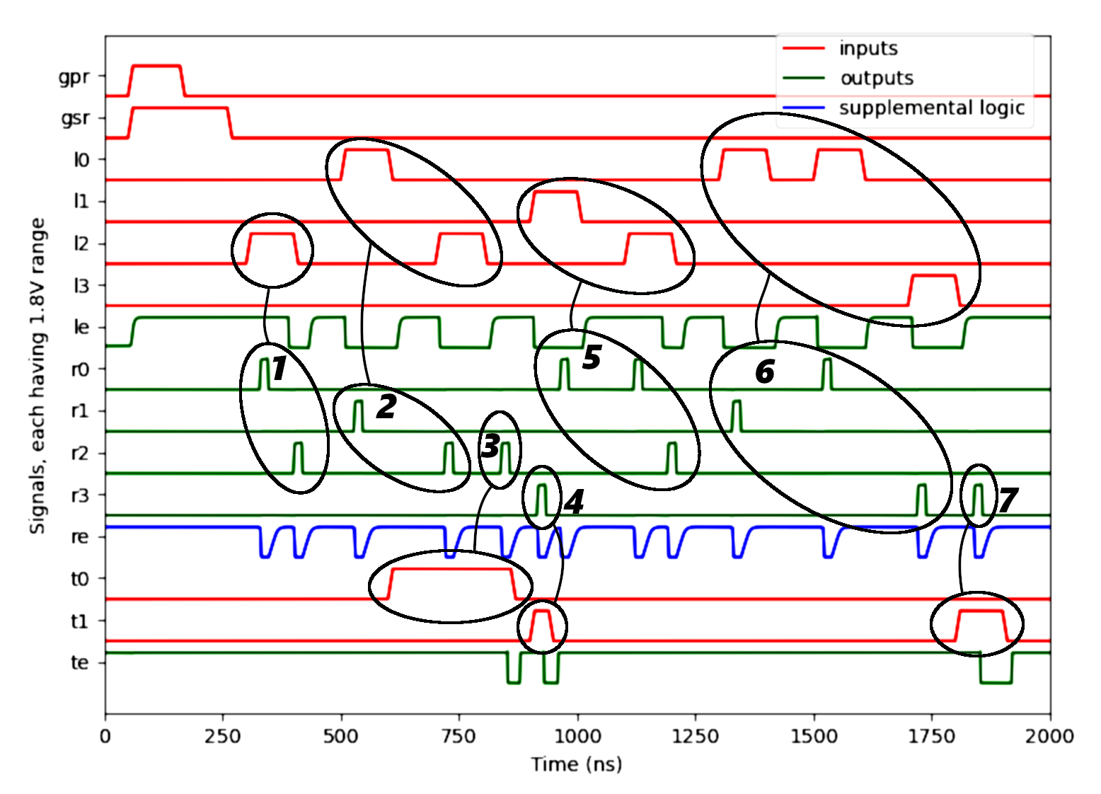
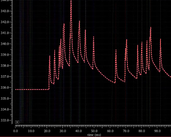
N-type-only circuits developed for event-based capacitive transduction, axonal and synaptic transmission, address-event multiplexing, and deep spiking neural networks, using Pragmatic FlexIC 800nm (simulation results).
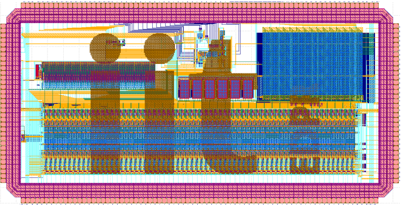
Design for wafer-scale integration with cross-linking and laser post-processing. The design was fabricated but could not be validated due to post-processing difficulties.
The design nevertheless helped us to explore the kinds of integration which might be possible.

Neuromorphic circuit designs supplied to Glasgow university for attempted integration with silicon nanowires.
The attempt failed at a mask-alignment step.
A wafer design with CNR (Rome) with many circuit primitives for CMOS integration via physical vapour deposition of organic semiconductor on a flexible substrate.
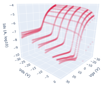
P-type transistors successful but N-type transistors failed. OFET characteristics dataset released. Some simple circuit primitives demonstrated.
Advisory role in Purdue OFET spiking neuron.